Mostrando entradas con la etiqueta Orozco Quiroz Deivid G.. Mostrar todas las entradas

sábado, 13 de febrero de 2010

Secrets Of Mosfet Cross Reference and Replacement Guide

mosfet cross reference

A Semiconductor Replacement Guide
Searching for the right mosfet cross reference or datasheet, one has to look for a semiconductor transistor replacement data book and not the Philip ECG master replacement guide. Almost all the transistor replacement book will published out the specification of a particular components such as type of component it belong whether it is a fet, scr, bipolar transistor, horizontal output transistor and also the voltage, ampere, wattage, ohm, frequency and suggested substitution part number.

From my experienced, the substitution part number that was recommended by the data book is not always 100 % match. If you have the time, I would like to suggest to you that, find the right part number by yourself rather than depending on the transistor data book.

It is the same when you look for horizontal output transistor (HOT) specification which doesn't mean that the bigger specification, the better the substitution part number is. In searching for Mosfet cross reference, you have to look at the ohms value which is provided by the transistor data book besides the specification of voltage, ampere and the wattage. The replacement, besides the same or higher in voltage, ampere and wattage, one should also consider the ohms value. The ohms value has to be as close as possible.

mosfet replacement

Arrow is showing the mosfet ohms value in a transistor substituion book

If the original fet part number is 1 ohm then a good replacement mosfet must have the ohm values between of 0.5 to 1.5 ohm. Do not substitute it with a too high or too low ohms value as this will make the mosfet run warmer and eventually blow the mosfet itself. Even though you can get a replacement with a higher voltage, ampere and wattage, if the ohms value is too low or too high, the mosfet will still burnt after on for quite a while.

True case study- An Epson inkjet printer sent in for repair with the complaint of no power. Checking the switch mode power supply found the power mosfet shorted. I don't have the original part number at my work place so I substitute it with a mosfet with a higher voltage, ampere and wattage and a higher ohm value than the original one with the help of my transistor cross reference guide.

It runs well for sometimes before it breakdown again. After two weeks the customer brought back the printer with the same complaint which is no power. Upon checking the power side I found the same mosfet gave up again. Substituting with another mosfet part number that have a similar specification especially the ohms value solved the printer no power symptom.

Specification with larger voltage, ampere and wattage don't guarantee that the replacement mosfet will work. So, taking the mosfet ohms value into consideration, you will have a higher chances to repaired the equipment and sometimes the replacement mosfet will also last longer.

Nombre:Orozco Q. Deivid G.
Asignatura: E.E.S
Fuente:www.electronicrepairguide.com


Explore the seven wonders of the world Learn more!

Mosfet Testing Tips-Test Fet with Analog Multimeter


testing mosfet


The right way of testing mosfet transistor is to use an analog multimeter. Mosfet stand for Metal oxide semiconductor field effect transistor or we just called it fet. Switch mode power supply and many other circuits uses fet transistors as part of a circuit. Mosfet failure and leakage are quite high in a circuit and you need to know how to accurately test it.

Measuring component's that have two leads such as the resistors, capacitors and diodes are much easier than measuring transistor and fet which have three legs. Many electronic repairers have difficulty especially checking the three leads components. First, find out the gate, drain and source pinout from semiconductor replacement book or search its datasheet from search engine.

Once you have the cross reference or diagram for each pin of the mosfet, then use your analogue multimeter set to times 10K ohm range to check it. Assuming you are testing the n channel mosfet then put the black probe to the drain pin.

Touch the gate pin with the red probe to discharge any internal capacitance in the mosfet. Now move the red probe to source pin while the black probe still touching the drain pin. Use your right finger and touch the gate and drain pin together and you will notice the analogue multimeter pointer will move forward to center range of the meter's scale.

 test fet

Use your finger to touch on the gate and drain pin.


Lifting the red probe from the source pin and putting it back again to the source pin, the pointer will still remain at the middle of the meter's scale. To discharge it you have to lift the red probe and touch just one time on the gate pin. This will eventually discharge the internal capacitance again.

At this time, use the red probe to touch on the source pin again, the pointer would not kick at all because you have already discharge it by touching the gate pin. These are the good mosfet characteristic.You need to practice more by taking some fet from your bench or from your component's compartment. Once you know the secrets, testing other mosfet is as simple as testing diode.

If you notice that all the result that you measured kicked towards zero ohms and will not discharge, then the fet is considered shorted and need replacement. Testing the P channel fet field effect transistor is just the same way as when you check N channel fet. What you do is to switch the probe polarity when checking the P channel. Some analog multimeter have the times 100k Ohm range, this type of meter can't really test fet due to the absent of 9 Volt battery inside the multimeter. This type of meter will not have enough power to trigger the mosfet. Make sure you use a meter that have the times 10k ohm range selector.

Typical N channel mosfet part numbers are 2SK791, K1118, IRF634, IRF 740 and P channel fet transistor part number are J307, J516, IRF 9620 and etc. You can also get a mosfet tester from the market and one of the famous brand is the sencore tf46 portable super cricket transistor and fet tester.

sencore fet tester

 Nombre:Orozco Q. Deivid G.
Asignatura: E.E.S.
Fuente:www.electronicrepairguide.com 


Discover the new Windows Vista Learn more!

MOS Capacitors

Structure and principle of operation
1. Flatband diagram
2. Accumulation
3. Depletion
4. Inversion

The MOS capacitor consists of a Metal-Oxide-Semiconductor structure as illustrated by Figure 1. Shown is the semiconductor substrate with a thin oxide layer and a top metal contact, referred to as the gate. A second metal layer forms an Ohmic contact to the back of the semiconductor and is called the bulk contact. The structure shown has a p-type substrate. We will refer to this as an n-type MOS or nMOS capacitor since the inversion layer - as discussed in section 4 - contains electrons.


Figure 1: MOS capacitance structure

To understand the different bias modes of an MOS capacitor we now consider three different bias voltages. One below the flatband voltage, VFB, a second between the flatband voltage and the threshold voltage, VT, and finally one larger than the threshold voltage. These bias regimes are called the accumulation, depletion and inversion mode of operation. These three modes as well as the charge distributions associated with each of them are shown in Figure 2.


Figure 2.: Charges in an n-type Metal-Oxide-Semiconductor structure (p-type substrate) under accumulation, depletion and inversion conditions.

Accumulation occurs typically for negative voltages where the negative charge on the gate attracts holes from the substrate to the oxide-semiconductor interface. Depletion occurs for positive voltages. The positive charge on the gate pushes the mobile holes into the substrate. Therefore, the semiconductor is depleted of mobile carriers at the interface and a negative charge, due to the ionized acceptor ions, is left in the space charge region. The voltage separating the accumulation and depletion regime is referred to as the flatband voltage, VFB. Inversion occurs at voltages beyond the threshold voltage. In inversion, there exists a negatively charged inversion layer at the oxide-semiconductor interface in addition to the depletion-layer. This inversion layer is due to the minority carriers that are attracted to the interface by the positive gate voltage.
The energy band diagram of an n-MOS capacitor biased in inversion is shown in Figure 3. The oxide is modeled as a semiconductor with a very large bandgap and blocks any flow of carriers between the semiconductor and the gate metal. The band bending in the semiconductor is consistent with the presence of a depletion layer. At the semiconductor-oxide interface, the Fermi energy is close to the conduction band edge as expected when a high density of electrons is present. The semiconductor remains in thermal equilibrium even when a voltage is applied to the gate. The presence of an electric field does not automatically lead to a non-equilibrium condition, as was also the case for a p-n diode with zero bias.


Figure 3.: Energy band diagram of an MOS structure biased in inversion.
In the next sections, we discuss the four modes of operation of an MOS structure: Flatband, Depletion, Inversion and Accumulation. Flatband conditions exist when no charge is present in the semiconductor so that the silicon energy band is flat. Initially we will assume that this occurs at zero gate bias. Later we will consider the actual flatband voltage in more detail. Surface depletion occurs when the holes in the substrate are pushed away by a positive gate voltage. A more positive voltage also attracts electrons (the minority carriers) to the surface, which form the so-called inversion layer. Under negative gate bias, one attracts holes from the p-type substrate to the surface, yielding accumulation.

1. Flatband diagram

 
The flatband diagram is by far the easiest energy band diagram. The term flatband refers to fact that the energy band diagram of the semiconductor is flat, which implies that no charge exists in the semiconductor. The flatband diagram of an aluminum-silicon dioxide-silicon MOS structure is shown in Figure 6.2.4. Note that a voltage, VFB, must be applied to obtain this flat band diagram. Indicated on the figure is also the work function of the aluminum gate, FM, the electron affinity of the oxide, coxide, and that of silicon, c, as well as the bandgap energy of silicon, Eg. The bandgap energy of the oxide is quoted in the literature to be between 8 and 9 electron volt. The reader should also realize that the oxide is an amorphous material and the use of semiconductor parameters for such material can justifiably be questioned.
The flatband voltage is obtained when the applied gate voltage equals the workfunction difference between the gate metal and the semiconductor. If there is a fixed charge in the oxide and/or at the oxide-silicon interface, the expression for the flatband voltage must be modified accordingly.


Figure 4: Flatband energy diagram of a metal-oxide-semiconductor (MOS) structure consisting of an aluminum metal, silicon dioxide and silicon.


2. Accumulation

Accumulation occurs when one applies a voltage less than the flatband voltage. The negative charge on the gate attracts holes from the substrate to the oxide-semiconductor interface. Only a small amount of band bending is needed to build up the accumulation charge so that almost all of the potential variation is within the oxide.

3. Depletion

As a more positive voltage than the flatband voltage is applied, a negative charge builds up in the semiconductor. Initially this charge is due to the depletion of the semiconductor starting from the oxide-semiconductor interface. The depletion layer width further increases with increasing gate voltage.

4. Inversion

As the potential across the semiconductor increases beyond twice the bulk potential, another type of negative charge emerges at the oxide-semiconductor interface: this charge is due to minority carriers, which form a so-called inversion layer. As one further increases the gate voltage, the depletion layer width barely increases further since the charge in the inversion layer increases exponentially with the surface potential.

Nombre:Orozco Quiroz Deivid G.
Asignatura:E.E.S
Fuente:ecee.colorado.edu


Explore the seven wonders of the world Learn more!

MOSFET DE CANAL CORTO

Mosfet de canal corto se define cuando el largo de la compuerta es del mismo orden de magnitud que el espesor de de su zona de deplexión en la unión fuente-drenador. Así que el Mosfet de canal corto (alternativamente) se puede definir cuando el largo efectivo del canal es aproximadamente igual a la profundidad de la unión fuente-drenador, o cuando el largo de su canal es menor que .

'Transistores'


Velocidad de saturación

El campo eléctrico se incrementa cuando el largo de la puerta disminuye. Como la velocidad de amontonamiento de electrones es proporcional a los campos eléctricos perpendiculares a la compuerta. Dicha velocidad aumenta . Por lo tanto la corriente en el canal se satura. Cuando se aproxima a , la velocidad de saturación electrónica . Esta saturación puede tener un gran impacto en las características voltaje-corriente. Considere la corriente drenador-fuente , de un Mosfet en saturación .


La corriente de saturación usando esta ecuación es menor que si usaremos la ecuación de un Mosfet de canal largo para . La corriente de saturación ya no será una función cuadrática de independientemente del largo del canal. La siguiente tabla muestra los valores de basados en la velocidad de saturación.

'Transistores'

VOLTAJE DE UMBRAL
Dependencia del largo del canal
La disminución de es un claro indicador de los efectos de canal corto. Graficando en el eje x y en el eje y, es notorio que hay una caída en el grafico.
El grafico indica que el mínimo que seria aceptable. La caída de es una de las consecuencias mas serias de los efectos de canal corto. La figura muestra demuestra este planteamiento.
'Transistores'
El voltaje de umbral no puede seguir el largo de compuerta en su descenso. El subvoltaje de umbral es inversamente proporcional a . Para transistores menores de 0.25um deben balancearse la velocidad y el bajo consumo de energía.
Como el largo del canal es menor que 2um, la aproximación de canal largo para el voltaje de umbral no es precisa. El generalmente disminuye con el largo de la compuerta (Vt rool-off).
También, el diminuye cuando se incrementa Vds. In orden para predecir el voltaje de umbral para un dispositivo de canal corto, el diferencial de debe ser aproximado. El efecto de canal corto (SCE) es por la formula siguiente, donde es el voltaje de umbral de canal largo.
La siguiente formula es útil para calcular la uniformidad y el dopaje de los canales:
Donde:
Es el grosor del oxido.
Es el ancho máximo de la zona deplexión debajo de la compuerta.
Es el largo de la zona de deplexión compuerta-fuente.

DIBL (Drain Induced Barrier Lowering) fue introducido en 1979 por Troutman. Como la caída de voltaje entre la fuente y el drenador se incrementa, la zona de deplexión bajo el drenador la barrera de potencial puede ser menor de potencial que la de unión de fuete al canal.
Si la barrera entre fuente y canal es disminuida los electrones tendrán mayor libertad para ser inyectados en la región del canal. Por tanto el voltaje disminuye y la compuerta tendrá menos control sobre la corriente del canal (ver fig. siguiente).
'Transistores'
DIBL
'Transistores'
Contra para dos diferentes largos de canal.

Dependencias del ancho de canal

Otro efecto sobre el voltaje de umbral ocurre cuando el ancho del canal es escalado. Los efectos de escalado del ancho de canal no son tan drásticos como los efectos de largo de canal. Existen 3 efectos producidos por el escalamiento del ancho de canal.
El primer efecto considera la región de deplexión perpendicular al flujo de corriente de fuente a drenador, a lo largo de la orilla de la compuerta en dirección del largo del canal. El campo eléctrico causa la deplexión la dirección vertical y consecuentemente también en la dirección lateral. La zona de deplexión paralela al flujo de corriente de fuente a drenador, lo que disminuirá el voltaje de umbral. Aunque la otra zona de deplexión causa que el voltaje de umbral aumente. La densidad de la carga en el canal es más grande cuando consideramos la carga de la región vertical y lateral.
'Transistores'

  • proceso de oxidación y elevación del campo eléctrico.

  • Proceso LOCOS semiresumido.


  • El segundo efecto va mas allá estrechando el canal, deteniendo el dopaje bajo los lados de la orilla de la compuerta paralelo al la dirección del largo del canal. El estrechamiento causa que haya más dopaje en los bordes que en el centro de la compuerta. Cuando esto sucede, se necesita un voltaje de compuerta mayor para invertir el canal.
    El tercer efecto ocurre cuando el silicón es removido totalmente próximo a la compuerta en dirección de L. Los otros 2 efectos no ocurren si el silicón no se agota. Cuando el silicón es removido próximo a la compuerta, mezclado con un dieléctrico es llamado barrera de aislamiento superficial (STI).
    'Transistores'
    (a) Contours of equipotentials and electron concentrations for an STI processed MOSFET.
    (b) I-V plot of the inverse narrow-width effect, which illustrates the hump in the subthreshold slope.


  • Proceso Básico De Fabricación De Mosfet De Canal Corto


  • Oxidación; oxidación de campo, oxidación de compuerta (en MOSFET).

  • Difusión, implantación de iones para dopaje de impurezas.

  • Proceso fotolitografico de estampado.

  • Insertado del dieléctrico, de metal o silicio, por solución química o plasma.

  • Deposición del silicio policristalino, oxido de silicón, nitrito de silicón, por deposición química de vapor (CVD).

  • Deposición de la capa de metal por calentamiento, o por evaporación electrónica y chipoteado.
    Paralelamente a este proceso se contrarrestan los efectos de canal corto con diversas innovaciones la fabricación en los mosfet.


  • Diferencias fundamentales entre Mosfet de canal corto
    Y
    Mosfet de canal largo


  • Los mosfet de canal corto tienen mayor frecuencia de operación que los Mosfet de canal largo.

  • Los mosfet de canal corto tienen mayor complejidad de fabricación que los mosfet de canal largo.

  • Los mosfet de canal largo tienen mayores dimensiones que los mosfet de canal corto.

  • Los mosfet de canal largo tienen mayores capacitáncias que los mosfet de canal corto.

  • Los mosfet de canal corto tienen mayor densidad que los mosfet de canal largo.

  • Los mosfet de canal corto tienen menor disipación de potencia.


  • Aplicaciones de los mosfet de canal corto


  • Dispositivos electrónicos que requieren altos niveles de integración, como microprocesadores (Pentium, AMD, Cyrix), chips de memoria DDR y DRAM (Kingston y Corsair).

  • Aplicaciones de alta frecuencia, debido a que su arquitectura permite el diseño de dispositivos más precisos.

  • Fabricantes de chipsets y motherboards (ASUS, DFI, SOYO, SIS) usan dispositivos CMOS porque ofrecen mayor flexibilidad, sobretodo en las memorias ROM, en el BIOS, y el resto del sistema.


  • Nombre:Orozco Quiroz Deivid G.
    Asignatura:E.E.S
    Fuente:www.rincondelvago.com


    Explore the seven wonders of the world Learn more!

    MOSFET scaling

    Over the past decades, the MOSFET has continually been scaled down in size; typical MOSFET channel lengths were once several micrometres, but modern integrated circuits are incorporating MOSFETs with channel lengths of tens of nanometers. Intel began production of a process featuring a 32 nm feature size (with the channel being even shorter) in late 2009. The semiconductor industry maintains a "roadmap", the ITRS [22], which sets the pace for MOSFET development. Historically, the difficulties with decreasing the size of the MOSFET have been associated with the semiconductor device fabrication process, the need to use very low voltages, and with poorer electrical performance necessitating circuit redesign and innovation (small MOSFETs exhibit higher leakage currents, and lower output resistance, discussed below).

    Reasons for MOSFET scaling
    Smaller MOSFETs are desirable for several reasons. The main reason to make transistors smaller is to pack more and more devices in a given chip area. This results in a chip with the same functionality in a smaller area, or chips with more functionality in the same area. Since fabrication costs for a semiconductor wafer are relatively fixed, the cost per integrated circuits is mainly related to the number of chips that can be produced per wafer. Hence, smaller ICs allow more chips per wafer, reducing the price per chip. In fact, over the past 30 years the number of transistors per chip has been doubled every 2–3 years once a new technology node is introduced. For example the number of MOSFETs in a microprocessor fabricated in a 45 nm technology is twice as large as in a 65 nm chip. This doubling of the transistor count was first observed by Gordon Moore in 1965 and is commonly referred to as Moore's law.[23]

    Trend of Intel CPU transistor gate lengthIt is also expected that smaller transistors switch faster. For example, one approach to size reduction is a scaling of the MOSFET that requires all device dimensions to reduce proportionally. The main device dimensions are the transistor length, width, and the oxide thickness, each (used to) scale with a factor of 0.7 per node. This way, the transistor channel resistance does not change with scaling, while gate capacitance is cut by a factor of 0.7. Hence, the RC delay of the transistor scales with a factor of 0.7.

    While this has been traditionally the case for the older technologies, for the state-of-the-art MOSFETs reduction of the transistor dimensions does not necessarily translate to higher chip speed because the delay due to interconnections is more significant.


    Difficulties arising due to MOSFET size reduction

    Producing MOSFETs with channel lengths much smaller than a micrometer is a challenge, and the difficulties of semiconductor device fabrication are always a limiting factor in advancing integrated circuit technology. In recent years, the small size of the MOSFET, below a few tens of nanometers, has created operational problems.
    Higher subthreshold conduction

    As MOSFET geometries shrink, the voltage that can be applied to the gate must be reduced to maintain reliability. To maintain performance, the threshold voltage of the MOSFET has to be reduced as well. As threshold voltage is reduced, the transistor cannot be switched from complete turn-off to complete turn-on with the limited voltage swing available; the circuit design is a compromise between strong current in the "on" case and low current in the "off" case, and the application determines whether to favor one over the other. Subthreshold leakage (including subthreshold conduction, gate-oxide leakage and reverse-biased junction leakage), which was ignored in the past, now can consume upwards of half of the total power consumption of modern high-performance VLSI chips.

    Increased gate-oxide leakage

    The gate oxide, which serves as insulator between the gate and channel, should be made as thin as possible to increase the channel conductivity and performance when the transistor is on and to reduce subthreshold leakage when the transistor is off. However, with current gate oxides with a thickness of around 1.2 nm (which in silicon is ~5 atoms thick) the quantum mechanical phenomenon of electron tunneling occurs between the gate and channel, leading to increased power consumption.

    Insulators (referred to as high-k dielectrics) that have a larger dielectric constant than silicon dioxide, such as group IVb metal silicates e.g. hafnium and zirconium silicates and oxides are being used to reduce the gate leakage from the 45 nanometer technology node onwards. Increasing the dielectric constant of the gate dielectric allows a thicker layer while maintaining a high capacitance (capacitance is proportional to dielectric constant and inversely proportional to dielectric thickness). All else equal, a higher dielectric thickness reduces the quantum tunneling current through the dielectric between the gate and the channel. On the other hand, the barrier height of the new gate insulator is an important consideration; the difference in conduction band energy between the semiconductor and the dielectric (and the corresponding difference in valence band energy) also affects leakage current level. For the traditional gate oxide, silicon dioxide, the former barrier is approximately 8 eV. For many alternative dielectrics the value is significantly lower, tending to increase the tunneling current, somewhat negating the advantage of higher dielectric constant.

    Increased junction leakage

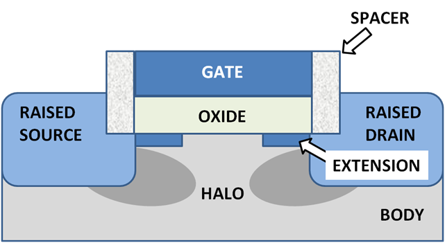
    To make devices smaller, junction design has become more complex, leading to higher doping levels, shallower junctions, "halo" doping and so forth, all to decrease drain-induced barrier lowering (see the section on junction design). To keep these complex junctions in place, the annealing steps formerly used to remove damage and electrically active defects must be curtailed[29] increasing junction leakage. Heavier doping is also associated with thinner depletion layers and more recombination centers that result in increased leakage current, even without lattice damage.

    Lower output resistance

    For analog operation, good gain requires a high MOSFET output impedance, which is to say, the MOSFET current should vary only slightly with the applied drain-to-source voltage. As devices are made smaller, the influence of the drain competes more successfully with that of the gate due to the growing proximity of these two electrodes, increasing the sensitivity of the MOSFET current to the drain voltage. To counteract the resulting decrease in output resistance, circuits are made more complex, either by requiring more devices, for example the cascode and cascade amplifiers, or by feedback circuitry using operational amplifiers.

    Lower transconductance

    The transconductance of the MOSFET decides its gain and is proportional to hole or electron mobility (depending on device type), at least for low drain voltages. As MOSFET size is reduced, the fields in the channel increase and the dopant impurity levels increase. Both changes reduce the carrier mobility, and hence the transconductance. As channel lengths are reduced without proportional reduction in drain voltage, raising the electric field in the channel, the result is velocity saturation of the carriers, limiting the current and the transconductance.

    Interconnect capacitance

    Traditionally, switching time was roughly proportional to the gate capacitance of gates. However, with transistors becoming smaller and more transistors being placed on the chip, interconnect capacitance (the capacitance of the wires connecting different parts of the chip) is becoming a large percentage of capacitance. Signals have to travel through the interconnect, which leads to increased delay and lower performance.

    Heat production

    Large heatsinks to cool power transistors in a TRM-800 audio amplifierThe ever-increasing density of MOSFETs on an integrated circuit is creating problems of substantial localized heat generation that can impair circuit operation. Circuits operate slower at high temperatures, and have reduced reliability and shorter lifetimes. Heat sinks and other cooling methods are now required for many integrated circuits including microprocessors.

    Power MOSFETs are at risk of thermal runaway. As their on-state resistance rises with temperature, if the load is approximately a constant-current load then the power loss rises correspondingly, generating further heat. When the heatsink is not able to keep the temperature low enough, the junction temperature may rise quickly and uncontrollably, resulting in destruction of the device.


    Process variations

    With MOSFETS becoming smaller, the number of atoms in the silicon that produce many of the transistor's properties is becoming fewer, with the result that control of dopant numbers and placement is more erratic. During chip manufacturing, random process variations affect all transistor dimensions: length, width, junction depths, oxide thickness etc., and become a greater percentage of overall transistor size as the transistor shrinks. The transistor characteristics become less certain, more statistical. The random nature of manufacture means we do not know which particular example MOSFETs actually will end up in a particular instance of the circuit. This uncertainty forces a less optimal design because the design must work for a great variety of possible component MOSFETs. See design for manufacturability, reliability engineering, six sigma and statistical process control.

    Modeling challenges

    Modern ICs are computer-simulated with the goal of obtaining working circuits from the very first manufactured lot. As devices are miniaturized, the complexity of the processing makes it difficult to predict exactly what the final devices look like, and modeling of physical processes becomes more challenging as well. In addition, microscopic variations in structure due simply to the probabilistic nature of atomic processes require statistical (not just deterministic) predictions. These factors combine to make adequate simulation and "right the first time" manufacture difficult.


    Nombre:Orozco Quiroz Deivid G.
    Asignatura:E.E.S
    Fuente:en.wikipedia.org


    Get news, entertainment and everything you care about at Live.com. Check it out!

    miércoles, 10 de febrero de 2010

    MOSFET Drain Current and Source

    Triode mode or linear region (also known as the ohmic mode)
    When VGS > Vth and VDS < ( VGS - Vth )
     
    The transistor is turned on, and a channel has been created which allows current to flow between the drain and the source. The MOSFET operates like a resistor, controlled by the gate voltage relative to both the source and drain voltages. The current from drain to source is modeled as:


    where μn is the charge-carrier effective mobility, W is the gate width, L is the gate length and Cox is the gate oxide capacitance per unit area. The transition from the exponential subthreshold region to the triode region is not as sharp as the equations suggest.

    Saturation or active mode
    When VGS > Vth and VDS > ( VGS - Vth )
     
    The switch is turned on, and a channel has been created, which allows current to flow between the drain and source. Since the drain voltage is higher than the gate voltage, the electrons spread out, and conduction is not through a narrow channel but through a broader, two- or three-dimensional current distribution extending away from the interface and deeper in the substrate. The onset of this region is also known as pinch-off to indicate the lack of channel region near the drain. The drain current is now weakly dependent upon drain voltage and controlled primarily by the gate-source voltage, and modeled very approximately as:

       
    The additional factor involving λ, the channel-length modulation parameter, models current dependence on drain voltage due to the Early effect, or channel length modulation. According to this equation, a key design parameter, the MOSFET transconductance is:
    ,

    where the combination Vov = VGS - Vth is called the overdrive voltage. Another key design parameter is the MOSFET output resistance rO given by:

    .
    If λ is taken as zero, an infinite output resistance of the device results that leads to unrealistic circuit predictions, particularly in analog circuits.
    As the channel length becomes very short, these equations become quite inaccurate. New physical effects arise. For example, carrier transport in the active mode may become limited by velocity saturation. When velocity saturation dominates, the saturation drain current is more nearly linear than quadratic in VGS. At even shorter lengths, carriers transport with near zero scattering, known as quasi-ballistic transport. In addition, the output current is affected by drain-induced barrier lowering of the threshold voltage.
    Nombre: Orozco Quiroz Deivid G.
    Asignatura: E.E.S.
    Fuente:en.wikipedia.org


    Explore the seven wonders of the world Learn more!

    Power MOSFET

    Cross section of a Power MOSFET, with square cells. A typical transistor is constituted of several thousand cellsMain article: Power MOSFET
    Power MOSFETs have a different structure than the one presented above.[35] As with all power devices, the structure is vertical and not planar. Using a vertical structure, it is possible for the transistor to sustain both high blocking voltage and high current. The voltage rating of the transistor is a function of the doping and thickness of the N-epitaxial layer (see cross section), while the current rating is a function of the channel width (the wider the channel, the higher the current). In a planar structure, the current and breakdown voltage ratings are both a function of the channel dimensions (respectively width and length of the channel), resulting in inefficient use of the "silicon estate". With the vertical structure, the component area is roughly proportional to the current it can sustain, and the component thickness (actually the N-epitaxial layer thickness) is proportional to the breakdown voltage.
    It is worth noting that power MOSFETs with lateral structure are mainly used in high-end audio amplifiers. Their advantage is a better behaviour in the saturated region (corresponding to the linear region of a bipolar transistor) than the vertical MOSFETs. Vertical MOSFETs are designed for switching applications.


    DMOS

    DMOS stands for double-diffused metal–oxide–semiconductor. Most of the power MOSFETs are made using this technology.

    RHBD MOSFETs

    Semiconductor sub-micron and nano-meter electronic circuits are the primary concern for operating within the normal tolerance in harsh radiation environments like space. One of the design approaches for making a radiation-hardened-by-design (RHBD) device is Enclosed-Layout-Transistor (ELT). Normally, the gate of the MOSFET surrounds the drain, which is placed in the center of the ELT. The source of the MOSFET surrounds the gate. Another RHBD MOSFET is called H-Gate. Both of these transistors have very low leakage current with respect to radiation. However, they are large in size and take more space on silicon than a standard MOSFET.
    Newer technologies are emerging for smaller devices for cost saving, low power and increased operating speed. The standard MOSFET is also becoming extremely sensitive to radiation for the newer technologies. A lot more research works should be completed before space electronics can safely use RHBD MOSFET circuits of nanotechnology.
    When radiation strikes near the silicon oxide region (STI) of the MOSFET, the channel inversion occurs at the corners of the standard MOSFET due to accumulation of radiation induced trapped charges. If the charges are large enough, the accumulated charges affect STI surface edges along the channel near the channel interface (gate) of the standard MOSFET. Thus the device channel inversion occurs along the channel edges and the device creates off-state leakage path, causing device to turn on. So the reliability of circuits degrades severely. The ELT offers many advantages. These advantages include improvement of reliability by reducing unwanted surface inversion at the gate edges that occurs in the standard MOSFET. Since the gate edges are enclosed in ELT, there is no gate oxide edge (STI at gate interface), and thus the transistor off-state leakage is reduced very much.
    Low-power microelectronic circuits including computers, communication devices and monitoring systems in space shuttle and satellites are very different than what we use on earth. They are radiation (high-speed atomic particles like proton and neutron, solar flare magnetic energy dissipation in earth's space, energetic cosmic rays like X-ray, Gamma-ray etc.) tolerant circuits. These special electronics are designed by applying very different techniques using RHBD MOSFETs to ensure the safe space journey and also space-walk of astronauts.


    Nombre: Orozco Quiroz Deivid G.
    Asignatura:E.E.S.
    Fuente:en.wikipedia.org


    Explore the seven wonders of the world Learn more!

    MOSFET construction

    Gate material

    The primary criterion for the gate material is that it is a good conductor. Highly-doped polycrystalline silicon is an acceptable but certainly not ideal conductor, and also suffers from some more technical deficiencies in its role as the standard gate material. Nevertheless, there are several reasons favoring use of polysilicon:
    • The threshold voltage (and consequently the drain to source on-current) is modified by work function the difference between the gate material and channel material. Because polysilicon is a semiconductor, its work function can be modulated by adjusting the type and level of doping. Furthermore, because polysilicon has the same bandgap as the underlying silicon channel, it is quite straightforward to tune the work function to achieve low threshold voltages for both NMOS and PMOS devices. By contrast, the work function of metals are not easily modulated, so tuning the work function to obtain low threshold voltages becomes a significant challenge. Additionally, obtaining low-threshold devices on both PMOS and NMOS devices would likely require the use of different metals for each device type, introducing additional complexity to the fabrication process.
    • The Silicon-SiO2 interface has been well studied and is known to have relatively few defects. By contrast many metal-insulator interfaces contain significant levels of defects which can lead to Fermi-level pinning, charging, or other phenomena that ultimately degrade device performance.
    • In the MOSFET IC fabrication process, it is preferable to deposit the gate material prior to certain high-temperature steps in order to make better-performing transistors. Such high temperature steps would melt some metals, limiting the types of metal that can be used in a metal-gate-based process.


    While polysilicon gates have been the de facto standard for the last twenty years, they do have some disadvantages which have led to their likely future replacement by metal gates. These disadvantages include:

    • Polysilicon is not a great conductor (approximately 1000 times more resistive than metals) which reduces the signal propagation speed through the material. The resistivity can be lowered by increasing the level of doping, but even highly doped polysilicon is not as conductive as most metals. In order to improve conductivity further, sometimes a high-temperature metal such as tungsten, titanium, cobalt, and more recently nickel is alloyed with the top layers of the polysilicon. Such a blended material is called silicide.. The silicide-polysilicon combination has better electrical properties than polysilicon alone and still does not melt in subsequent processing. Also the threshold voltage is not significantly higher than with polysilicon alone, because the silicide material is not near the channel. The process in which silicide is formed on both the gate electrode and the source and drain regions is sometimes called salicide, self-aligned silicide.
    • When the transistors are extremely scaled down, it is necessary to make the gate dielectric layer very thin, around 1 nm in state-of-the-art technologies. A phenomenon observed here is the so-called poly depletion, where a depletion layer is formed in the gate polysilicon layer next to the gate dielectric when the transistor is in the inversion. To avoid this problem, a metal gate is desired. A variety of metal gates such as tantalum, tungsten, tantalum nitride, and titanium nitride are used, usually in conjunction with high-k dielectrics. An alternative is to use fully-silicided polysilicon gates, a process known as FUSI.

    Insulator

    As devices are made smaller, insulating layers are made thinner, and at some point tunneling of carriers through the insulator from the channel to the gate electrode takes place. To reduce the resulting leakage current, the insulator can be made thicker by choosing a material with a higher dielectric constant. To see how thickness and dielectric constant are related, note that Gauss' law connects field to charge as:


    with Q = charge density, κ = dielectric constant, ε0 = permittivity of empty space and E = electric field. From this law it appears the same charge can be maintained in the channel at a lower field provided κ is increased. The voltage on the gate is given by:


    with VG = gate voltage, Vch = voltage at channel side of insulator, and tins = insulator thickness. This equation shows the gate voltage will not increase when the insulator thickness increases, provided κ increases to keep tins /κ = constant (see the article on high-κ dielectrics for more detail, and the section in this article on gate-oxide leakage).
    The insulator in a MOSFET is a dielectric which can in any event be silicon oxide, but many other dielectric materials are employed. The generic term for the dielectric is gate dielectric since the dielectric lies directly below the gate electrode and above the channel of the MOSFET.

    Junction design

    The source-to-body and drain-to-body junctions are the object of much attention because of three major factors: their design affects the current-voltage (I-V) characteristics of the device, lowering output resistance, and also the speed of the device through the loading effect of the junction capacitances, and finally, the component of stand-by power dissipation due to junction leakage.

    MOSFET showing shallow junction extensions, raised source and drain and halo implant. Raised source and drain separated from gate by oxide spacers.The drain induced barrier lowering of the threshold voltage and channel length modulation effects upon I-V curves are reduced by using shallow junction extensions. In addition, halo doping can be used, that is, the addition of very thin heavily doped regions of the same doping type as the body tight against the junction walls to limit the extent of depletion regions.
    The capacitive effects are limited by using raised source and drain geometries that make most of the contact area border thick dielectric instead of silicon.
    These various features of junction design are shown (with artistic license) in the figure.
    Junction leakage is discussed further in the section increased junction leakage.

    Nombre:Orozco Quiroz Deivid G.
    Asignatura:E.E.S.
    Fuente:en.wikipedia.org


    Connect to the next generation of MSN Messenger  Get it now!

    lunes, 8 de febrero de 2010

    MOSFET structure and channel formation

    MOSFET structure and channel formation

    Cross section of an NMOS without channel formed: OFF state


    Cross section of an NMOS with channel formed: ON stateA metal–oxide–semiconductor field-effect transistor (MOSFET) is based on the modulation of charge concentration by a MOS capacitance between a body electrode and a gate electrode located above the body and insulated from all other device regions by a gate dielectric layer which in the case of a MOSFET is an oxide, such as silicon dioxide. If dielectrics other than an oxide such as silicon dioxide (often referred to as oxide) are employed the device may be referred to as a metal–insulator–semiconductor FET (MISFET). Compared to the MOS capacitor, the MOSFET includes two additional terminals (source and drain), each connected to individual highly doped regions that are separated by the body region. These regions can be either p or n type, but they must both be of the same type, and of opposite type to the body region. The source and drain (unlike the body) are highly doped as signified by a '+' sign after the type of doping.


    If the MOSFET is an n-channel or nMOS FET, then the source and drain are 'n+' regions and the body is a 'p' region. As described above, with sufficient gate voltage, above a threshold voltage value, electrons from the source (and possibly[citation needed] also the drain) enter the inversion layer or n-channel at the interface between the p region and the oxide. This conducting channel extends between the source and the drain, and current is conducted through it when a voltage is applied between source and drain.

    For gate voltages below the threshold value, the channel is lightly populated, and only a very small subthreshold leakage current can flow between the source and the drain.

    If the MOSFET is a p-channel or pMOS FET, then the source and drain are 'p+' regions and the body is a 'n' region. When a negative gate-source voltage (positive source-gate) is applied, it creates a p-channel at the surface of the n region, analogous to the n-channel case, but with opposite polarities of charges and voltages. When a voltage less negative than the threshold value (a negative voltage for p-channel) is applied between gate and source, the channel disappears and only a very small subthreshold current can flow between the source and the drain.

    The source is so named because it is the source of the charge carriers (electrons for n-channel, holes for p-channel) that flow through the channel; similarly, the drain is where the charge carriers leave the channel.

    The device may comprise a Silicon On Insulator (SOI) device in which a Buried OXide (BOX) is formed below a thin semiconductor layer. If the channel region between the gate dielectric and a Buried OXide (BOX) region is very thin, the very thin channel region is referred to as an Ultra Thin Channel (UTC) region with the source and drain regions formed on either side thereof in and/or above the thin semiconductor layer. Alternatively, the device may comprise a SEMiconductor

    On Insulator (SEMOI) device in which other semiconductors than silicon are employed. Many alternative semicondutor materials may be employed.

    When the source and drain regions are formed above the channel in whole or in part, they are referred to as Raised Source/Drain (RSD) regions.

    Nombre: Orozco Quiroz Deivid G.
    Asignatura:E.E.S.
    Fuente:en.wikipedia.org


    Connect to the next generation of MSN Messenger  Get it now!

    Mosfet Acumulación y Deplexión

    Los MOSFET de acumulación


    Pasos para la fabricación de un transistor MOSFET

    Partiendo de un sustrato tipo N se forma sobre su superficie una fina capa de óxido. Empleando las técnicas de máscaras y corrosión se practican dos aberturas en dicha capa de óxido, a través de las cuales se difundirán impurezas tipo P. Con estas etapas de fabricación se llega al estado representado en la ilustración correspondiente. Las dos regiones P constituyen la fuente y el drenaje. Se forma una capa de óxido de mayor espesor sobre la superficie, en la que se practican tres aperturas mediante una segunda aplicación de las técnicas de máscara y corrosión; se añade, encima, una fina capa de SiO2, para el óxido de puerta. Con una tercera máscara se elimina el óxido que cubre las regiones de fuente y drenaje. Seguidamente, se cubre con aluminio vaporizado toda la superficie. Una última corrosión con máscara elimina el aluminio sobrante para suprimir las interconexiones entre fuente, puerta y drenaje.


    MOSFET de acumulacíón con canal tipo P

    Para analizar el funcionamiento de este tipo de transistores conectamos a tierra el sustrato y la fuente, es decir, hacemos que la tensión entre fuente y drenaje sea cero, y aplicamos una tensión negativa a la puerta. Se creará un campo eléctrico perpendicular al óxido, el cual inducirá cargas positivas junto a la superficie del semiconductor. Como el sustrato tipo N contiene muy pocos huecos, las cargas positivas superficiales son principalmente huecos procedentes de la fuente y el drenaje tipo P. Estas cargas móviles, que son portadores minoritarios en el sustrato, forman una capa de inversión sólo si la tensión fuente - puerta supera el nivel umbral. A medida que la tensión negativa de puerta sube por encima del umbral, las cargas positivas inducidas en el conductor también crecen. La región debajo del óxido es ahora un canal P, la conductividad aumenta y circula corriente desde la fuente al drenaje a través del canal inducido al aplicar un potencial negativo de drenaje y fuente. Por tanto, la corriente de drenaje se intensifica con la tensión negativa de puerta, por lo que el dispositivo recibe el nombre de MOSFET de acumulación.

    Los MOSFET de deplexión

    Si en la estructura básica de un transistor MOSFET se difunde un canal entre fuente y drenaje, con el mismo tipo de impurezas empleadas en la difusión de las propias fuente y drenaje, se obtiene el MOSFET de deplexión. Consideremos la estructura de canal N mostrada en la ilustración correspondiente. Si la tensión fuente-drenaje es positiva, circulará una apreciable corriente de drenaje para un tensión de puerta-fuente de cero voltios.


    MOSFET de deplexión con canal tipo N

    Si la tensión de puerta se hace negativa, se inducen cargas positivas en el canal a través del óxido del condensador de puerta. Puesto que la corriente en un transistor de efecto de campo es debida a los portadores mayoritarios (electrones en un material tipo N), las cargas inducidas positivas hacen el canal menos conductor y la corriente de drenaje cae cuando la tensión puerta - fuente se va haciendo más negativo. La redistribución de las cargas en el canal provoca una deplexión o debilitamiento efectivo de portadores mayoritarios, de ahí su nombre: "MOSFET de deplexión".

    Nombre:Orozco Quiroz Deivid G.
    Asignatura:E.E.S.
    Fuente:www.angelfire.com


    Get news, entertainment and everything you care about at Live.com. Check it out!

    Operación y construcción del MOSFET

    En esta sección, se considera el FET de metal –óxido semiconductor (MOSFET). Este FET se construye con la terminal de compuerta aislada del canal con el dielectrico dióxido de silicio (SiO2), y ya sea en modo de empobrecimiento o bien de enriquecimiento. Estos dos tipos se definen a continuación


    MOSFET de empobrecimiento

    Las construcciones de los MOSFET de empobrecimiento de canal n y de canal p. En cada una de estas figuras se muestra la construcción, el simbolo, la caracteristica de transferencia y las caracteristicas iD-vGS. El MOSFET de empobrecimiento se construye para el de canal n  con un canal fisico construido entre el drenaje y la fuente. Como resultado de ello, existe una iD entre drenaje y fuente cuando se aplica una tension, vDS.

    El MOSFET de empobrecimiento de canal n  se establece en un sustrato p, que es silicio contaminado de tipo p. Las regiones contaminadas de tipo n de la fuente y el drenaje forman conexiones de baja resistencia entre los extremos del canal n y los contactos de aluminio de la fuente (S) y el drenaje (D). Se hace crecer una capa de SiO2, que es un aislante, en la parte superior del canal n. Se deposita una capa de aluminio sobre el aislante de SiO2 para formar el material de compuerta (G). El desempeño del MOSFET de empobrecimiento, es similar al del JFET. El JFET se controla por la unión pn entre la compuerta y el extremo de drenaje del canal. No existe dicha unión en el MOSFET enriquecimiento, y la capa de SiO2 actúa como aislante. Para el MOSFET de canal n, una vGS negativa saca los electrones de la región del canal, empobreciéndolo. Cuando vGS alcanza VP, el canal se estrangula. Los valores positivos de vGS aumentan el tamaño del canal, dando por resultado un aumento en la corriente de drenaje.


    MOSFET de enriquecimiento

    El MOSFET de enriquecimiento difiere del MOSFET de empobrecimiento en que no tiene la capa delgada de material n sino que requiere de una tension positiva entre la compuerta y la fuente para establecer un canal. Este canal se forma por la acción de una tension positiva compuerta a fuente, vGS, que atrae electrones de la región de sustrato ubicada entre el drenaje y la compuerta contaminados de tipo n. Una vGS positiva provoca que los electrones se acumulen en la superficie inferior de la capa de oxido. Cuando la tensión alcanza el valor de umbral, VT, han sido atraidos a esta región los electrones suficientes para que se comporte como canal n conductor. No habra una corriente apreciable iD hasta que vGS excede VT.

    Nombre: Orozco Quiroz Deivid G.
    Asignatura: E.E.S


    Get news, entertainment and everything you care about at Live.com. Check it out!

    MOSFET: Metal Oxide Semiconductor Field Effect Transistor


    MOSFET MOSFET significa "FET de Metal Oxido Semiconductor" o FET de compuerta aislada


    Es un tipo especial de transistor FET que tiene una versión NPN y otra PNP.

    El NPN es llamado MOSFET de canal N y el PNP es llamado MOSFET de canal P.

    Una delgada capa de material aislante formada de dióxido de silicio (SiO2) (también llamada "sílice" o "sílica") es colocada del lado del semiconductor y una capa de metal es colocada del lado de la compuerta (GATE)

    En el MOSFET de canal N la parte "N" está conectado a la fuente (source) y al drenaje (drain)
    En el MOSFET de canal P la parte "P" está conectado a la fuente (source) y al drenaje (drain)
    En los transistores bipolares la corriente que circula por el colector es controlada por la corriente que circula por la base. Sin embargo en el caso de los transistores FET, la corriente de salida es controlada por una tensión de entrada (un campo eléctrico). En este caso no existe corriente de entrada.
    Los transistores MOSFET se pueden dañar con facilidad y hay que manipularlos con cuidado. Debido a que la capa de óxido es muy delgada, se puede destruir con facilidad si hay alta tensión o hay electricidad estática.

    MOSFET de canal N, construcción y símbolo  -  Electrónica Unicrom         MOSFET de canal P, construcción y símbolo  -  Electrónica Unicrom


    Principio de operación de un MOSFET

    Tanto en el MOSFET de canal N o el de canal P, cuando no se aplica tensión en la compuerta no hay flujo de corriente entre en drenaje (Drain) y la fuente (Source)

    MOSFET de canal N, principio de operación  -  Electrónica Unicrom            MOSFET de canal P, principio de operación  -  Electrónica Unicrom
               
    Para que circule corriente en un MOSFET de canal N una tensión positiva se debe aplicar en la compuerta. Así los electrones del canal N de la fuente (source) y el drenaje (Drain) son atraídos a la compuerta (Gate) y pasan por el canal P entre ellos.
    El movimiento de estos electrones, crea las condiciones para que aparezca un puente para los electrones entre el drenaje y la fuente. La amplitud o anchura de este puente (y la cantidad de corriente) depende o es controlada por la tensión aplicada a la compuerta.
    En el caso del MOSFET de canal P, se da una situación similar. Cuando se aplica una tensión negativa en la compuerta, los huecos (ausencia de electrones) del canal P del drenaje y de la fuente son atraídos hacia la compuerta y pasan a través del canal N que hay entre ellos, creando un puente entre drenaje y fuente. La amplitud o anchura del puente (y la cantidad de corriente) depende de la tensión aplicada a la compuerta.
    Debido a la delgada capa de óxido que hay entre la compuerta y el semiconductor, no hay corriente por la compuerta. La corriente que circula entre drenaje y fuente es controlada por la tensión aplicada a la compuerta.

    Nombre:Orozco Quiroz Deivid G.
    Asignatura: E.E.S.
    Fuente:www.unicrom.com


    Connect to the next generation of MSN Messenger  Get it now!