Gate material
The primary criterion for the gate material is that it is a good conductor. Highly-doped polycrystalline silicon is an acceptable but certainly not ideal conductor, and also suffers from some more technical deficiencies in its role as the standard gate material. Nevertheless, there are several reasons favoring use of polysilicon:
- The threshold voltage (and consequently the drain to source on-current) is modified by work function the difference between the gate material and channel material. Because polysilicon is a semiconductor, its work function can be modulated by adjusting the type and level of doping. Furthermore, because polysilicon has the same bandgap as the underlying silicon channel, it is quite straightforward to tune the work function to achieve low threshold voltages for both NMOS and PMOS devices. By contrast, the work function of metals are not easily modulated, so tuning the work function to obtain low threshold voltages becomes a significant challenge. Additionally, obtaining low-threshold devices on both PMOS and NMOS devices would likely require the use of different metals for each device type, introducing additional complexity to the fabrication process.
- The Silicon-SiO2 interface has been well studied and is known to have relatively few defects. By contrast many metal-insulator interfaces contain significant levels of defects which can lead to Fermi-level pinning, charging, or other phenomena that ultimately degrade device performance.
- In the MOSFET IC fabrication process, it is preferable to deposit the gate material prior to certain high-temperature steps in order to make better-performing transistors. Such high temperature steps would melt some metals, limiting the types of metal that can be used in a metal-gate-based process.
While polysilicon gates have been the de facto standard for the last twenty years, they do have some disadvantages which have led to their likely future replacement by metal gates. These disadvantages include:
- Polysilicon is not a great conductor (approximately 1000 times more resistive than metals) which reduces the signal propagation speed through the material. The resistivity can be lowered by increasing the level of doping, but even highly doped polysilicon is not as conductive as most metals. In order to improve conductivity further, sometimes a high-temperature metal such as tungsten, titanium, cobalt, and more recently nickel is alloyed with the top layers of the polysilicon. Such a blended material is called silicide.. The silicide-polysilicon combination has better electrical properties than polysilicon alone and still does not melt in subsequent processing. Also the threshold voltage is not significantly higher than with polysilicon alone, because the silicide material is not near the channel. The process in which silicide is formed on both the gate electrode and the source and drain regions is sometimes called salicide, self-aligned silicide.
- When the transistors are extremely scaled down, it is necessary to make the gate dielectric layer very thin, around 1 nm in state-of-the-art technologies. A phenomenon observed here is the so-called poly depletion, where a depletion layer is formed in the gate polysilicon layer next to the gate dielectric when the transistor is in the inversion. To avoid this problem, a metal gate is desired. A variety of metal gates such as tantalum, tungsten, tantalum nitride, and titanium nitride are used, usually in conjunction with high-k dielectrics. An alternative is to use fully-silicided polysilicon gates, a process known as FUSI.
Insulator
As devices are made smaller, insulating layers are made thinner, and at some point tunneling of carriers through the insulator from the channel to the gate electrode takes place. To reduce the resulting leakage current, the insulator can be made thicker by choosing a material with a higher dielectric constant. To see how thickness and dielectric constant are related, note that Gauss' law connects field to charge as:
with Q = charge density, κ = dielectric constant, ε0 = permittivity of empty space and E = electric field. From this law it appears the same charge can be maintained in the channel at a lower field provided κ is increased. The voltage on the gate is given by:
with VG = gate voltage, Vch = voltage at channel side of insulator, and tins = insulator thickness. This equation shows the gate voltage will not increase when the insulator thickness increases, provided κ increases to keep tins /κ = constant (see the article on high-κ dielectrics for more detail, and the section in this article on gate-oxide leakage).
The insulator in a MOSFET is a dielectric which can in any event be silicon oxide, but many other dielectric materials are employed. The generic term for the dielectric is gate dielectric since the dielectric lies directly below the gate electrode and above the channel of the MOSFET.
Junction design
The source-to-body and drain-to-body junctions are the object of much attention because of three major factors: their design affects the current-voltage (I-V) characteristics of the device, lowering output resistance, and also the speed of the device through the loading effect of the junction capacitances, and finally, the component of stand-by power dissipation due to junction leakage.
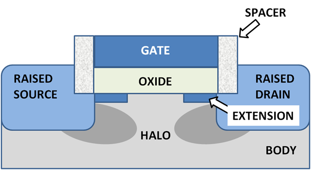
MOSFET showing shallow junction extensions, raised source and drain and halo implant. Raised source and drain separated from gate by oxide spacers.The drain induced barrier lowering of the threshold voltage and channel length modulation effects upon I-V curves are reduced by using shallow junction extensions. In addition, halo doping can be used, that is, the addition of very thin heavily doped regions of the same doping type as the body tight against the junction walls to limit the extent of depletion regions.
The capacitive effects are limited by using raised source and drain geometries that make most of the contact area border thick dielectric instead of silicon.
These various features of junction design are shown (with artistic license) in the figure.
Junction leakage is discussed further in the section increased junction leakage.
Nombre:Orozco Quiroz Deivid G.
Asignatura:E.E.S.
Fuente:en.wikipedia.org
Connect to the next generation of MSN Messenger Get it now!
No hay comentarios:
Publicar un comentario